| |
|
HP 82929A
Programmable ROM Drawer Clone
The HP 82929A Programmable ROM Drawer is one of the many accessory modules available
for the HP Series 80 personal computers.
The module fits into one of the rear expansion slots and allows you to add your own
code resident in PROM or EPROM, or any of the old original ROM modules for which images are
available on-line.
After removing the enclosure of the HP 82929A module you will find two 28-pin DIP
sockets that can accommodate either two 4KByte (2732) or two 8KByte (2764) EPROMs.
Each ROM module image is 8KBytes, then using 2764 EPROMs you can add two additional
ROM module images with the HP 82929A module.
Project Description
Given that the HP 28292A is one of the hard to find accessories to for the
HP Series 80 and it's a must have if you don't have some of the original
expansion ROMs such as the Assembler ROM, the primary goal of this project is
to design and build a functional clone of the HP 28292A.
The final goal is to be able to use a microcontroller to emulate the external
ROMs but use the microcontroller FLASH memory to hold single or multiple images
of the expansion ROMs (a similar approach was used to emulate the expansion
ROM cartridges for the HP-41 calculator).
|
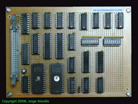
HP 82929A Clone Prototype
Top Side
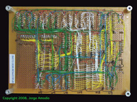
HP 82929A Clone Prototype
Bottom Side
[Click Images to Enlarge]
|
This project will have several phases.
The first phase is to design an equivalent circuit to the original HP 28292A
using off the shelf CMOS/TTL currently available components and build a prototype.
For this phase we will rely on the schematics obtained by
reverse engineering and actual HP 82929A module.
The second phase will be to gather detailed timing specifications and requirements
using the clone prototype as a test bed for the selection of an appropiate
microcontroller and basic architecture of a second generation clone prototype.
Third phase will be then to develop the microcontroller based clone and associated
firmware.
Project Progress
Based on the schematics obtained from the original HP 82929A board and a quick search
of available parts at Mouser Electronics,
Digikey and Jameco,
I put together a new schematic that has some minor modifications from the original:
- The bidirectional CD40166 (CMOS/TTL buffer/level translator) was replaced
by a pair of 74HC244 tri-state octal buffers.
- Instead of using 4 74LS161 4-bit binary counters that conform the Address Register
and counter, I used a pair of 74F269 8-bit binary counters that provide the same
functionality.
- As a replacement for the pair of AM25LS25121 8-bit identity comparators I used
a pair of 74ACT521 or you can also use 74LS688 which provide the same function.
- I didn't include an equivalent to the DM81LS96 present in the original design
since it's not necessary to invert the data lines and the EPROMs already provide
3-State functionality. I just then modified the connection to the Output Enable pin
of the EPROMs.
- I added two LEDs, one (red) to show the status of Vcc, and the other one (green)
to show when any of the two EPROMs are selected.
With the changes mentioned above I put together a first prototype board using standard
DIP parts and wirewrap sockets. The end product is shown in the two pictures on the
top right of this page.
The next step is to connect the prototype board to the HP-85 expansion slot and
test if everything works as expected. As you may have noticed the prototype board
has a 40-pin IDC connector, which is intended to be the connection to the
HP-85 expansion slot.
I've been thinking and working about different alternatives to connect this
prototype board and may be others to come to the HP-85. While I was doing some
research about the HP-85 bus signal I had one machine with a flat ribbon cable
coming out from the cabinet, each wire was soldered directly to the back of
one of the expansion slot edge connectors and on the other side terminated
on a long male pin header attached to a solderless breadboard.
This alternative was cheap and it worked but I was not very comfortable
(less having small kids hanging out in my office/lab daily) to leave the wires
permanently connected to the guts of the HP-85, and on the other hand I could
not move the connection to another machine (I've a small collection of HP Series 80
machines).
I designed different small boards with a card edge connector matching the
expansion slot of the HP-85, finally I decided to go with a version that has the 40-pin
IDC connector for the flat cable and pads for a pin header so I can use the same
board to terminate the flat cable on a solderless breadboard.
The following two pictures show how the pcb came out and fits on the I/O expansion
slot. Don't pay much attention to the cheap solder mask (actually is nail polish), also
I didn't have an IDC connector in angle then I'm sort of loosing at least one slot
but for prototyping purposes it really doesn't matter much.
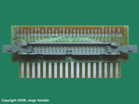
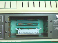
[Click Images to Enlarge]
As expected and applying
Murphy's law, the board didn't work on the first try.
I had an error in the schematic for the original module, the Chip Select signals
for the EEPROMs were permuted, and I also had few wiring mistakes.
Just to increase reliability I added pull-up resistors to the data outputs
of the EEPROMs. The previous design of an EEPROM board by HP for internal use
had pull-ups and a 80C97 three-state buffer that in this design is being
substituted by a 74HC244.
While troubleshooting I found that the RC (Read Control) signal is quite
sensitive to additional loading, such as the oscilloscope or the
logic analyzer probe.
After correcting the wiring errors and removing the extra load on the RC signal,
the thing worked very well, even with a longer flat cable of about 4 feet.
Below is a picture of the clone module being tested on a HP-85A with the
Assembler and Service ROM images on a pair of 27C64 EEPROMs.
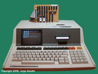
[Click Image to Enlarge]
I'm not sure yet if I'll invest the time to develop a pcb layout for this version
of the clone.
The link to the schematics pdf file now points to the corrected version (2.3).
Project Status
(as of 2/10/08)
- Clone prototype schematics and board layout - done
- Wired DIP parts prototype board - done
- Design and order bus expansion adapter pcb - done
- Make 40-pin to 40-pin flat cable - done
- Put together at least 2 adapters when the pcbs arrive - done
- Test the clone prototype with HP-85A - done
To Do List
- Test the clone prototype with HP-85B
- Test the clone prototype with HP-86B
- Test the clone prototype with HP-87XM
- Preliminary PCB design & costs with SMD parts (conditional)
- Explore if there is interest for a small pcb production batch
- Define specs and requirements for microcontroller based design
- Select microcontroller
- Develop microcontroller based design project plan
|
Useful links
|
|
|

