Description
The ENC28J60 is Microchip's first incursion into the ethernet controller arena,
this new device includes all MAC & PHY IEEE 802.3 10BaseT functions, 8KB of
dual access RAM packet buffer and a SPI serial interface, all in a convenient
28-pin package (SPDIP, SOIC, SSOP and QFN packages available).
It takes just few components to get the ENC28J60 up and running and connected to
a host microprocessor or microcontroller with support for the industry standard
SPI interface.
This project includes the schematics and related information for a simple
hardware implementation based on the ENC28J60 (ENC) and a Microchip PIC18F 8-bit
microcontroller running Microchip's free TCP/IP stack.
Design considerations
While a PIC18F452 MCU can be used for this project, a better and recommended
option due its additional program and RAM memory space is the PIC18F4620 (40-pin)
or the PIC18F2620 (28-pin) if fewer I/O interfaces are needed.
The ENC has 3.3V Vdd supply, one alternative is to use a MCU also with
3.3V Vdd (such as a PIC18LF4620) but depending on the MCU selection
this will limit the maximum clock frequency supported by the MCU then reducing
also the maximum SPI clock generated from the MCU clock.
Another alternative is to use 5V Vdd for the MCU, but in this case level
conversion is required for at least the signals from the ENC to the MCU,
no conversion is necessary on the other way since the ENC inputs are 5V
tolerant but a small (100-300ohms) resistor in series is recommended to reduce
undershoots.
|
 [Click Image to Enlarge]
 [Click Image to Enlarge]
 [Click Image to Enlarge]
|
Another consideration is that silicon revisions of the ENC28J60 prior to B5
have a bug that requires the SPI clock (SCK) to be between 8MHz to 10MHz to avoid
clock synchronization problems and unreliable access to the ENC registers,
then you have to choose a MCU clock speed that permits generating a SPI clock
within the acceptable range, or as a workaround to this problem use the same
clock source for both devices, for example using the ENC28J60 CLKOUT output
as the source for the MCU clock (this configuration is shown in the
miniPIC10T project that is a variant of
this project showing a minimal implementation).
This clock synchronization problem has been fixed in the B5 silicon revision,
the new acceptable range for SCK is now DC to 20MHz.
The new silicon revision introduced another change, now the recommended value for
RBIAS (R17 in the schematics) is 2.32K 1% for Rev B5 and 2.7K 1% for Rev B1/B4.
It's important that you use the correct value for RBIAS since it controls the
signal shape of the differential outputs, a wrong value can produce deformation
of the signal and non-compliance with IEEE 802.3.
For this project we will use a dual power supply, 5V for the MCU and a 3.3V
regulator for the ENC, a 74ACT125 or 74HCT125 3-state buffer for level
conversion, and a 10MHz can oscillator (a 10MHz parallel crystal works fine
too) with HS-PLL enabled for a MCU clock speed of 40MHz with SCK=Fosc/4 ie 10MHz.
The hardware design includes a 25LC256 serial EEPROM (the new 25LC1024 is also
supported) for storage of configuration information and web pages,
several leds, a RS232 driver for a serial interface, some push buttons and a
20x2 LCD character module (HD44780 or equivalent controller).
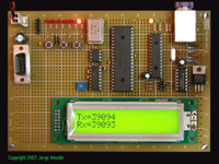
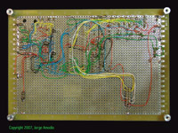
Several people asked if this type of circuit can be built using wire-wrap.
As you can see from the last picture on, the answer is yes, just keep your wires
as short as possible and flat to the board.
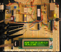
The first hardware prototype was built in a prototype breadboard shown in the
first picture from the top and then moved to a standard wire-wrapped prototype board.
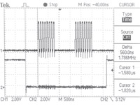
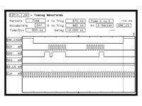
SPI Interface signals
For your reference, the two images below show an oscilloscope and logic analyzer screen
captures of various SPI signals.
|
[Click on the image for a larger view]
|
The image on the left is an oscilloscope capture showing SPI SCK in Channel 1 and ENC28J60
CS (Chip Select) in Channel 2. The image on the right is a logic analyzer capture showing
the ENC28J60 CS, all SPI signals (SCK, SDO, SDI), the 25LC256 Chip Select and the MCU
clock at 10MHz.
|
Getting the board up and running
Compiling the firmware is not a huge or complicated task, it requires few
software tools available for download from Microchip's
website at no cost, and obviously the TCP/IP stack source code distribution and a
PIC programmer. For this project I used Microchip's
MPLAB ICD2 as a programmer.
With the latest modified version of the
Microchip TCP/IP Stack v3.75, the process is quite simple.
This new version adds the PIC10T macro definition that
combined with the device selection for the Microcontroller generates the appropriate
code for this particular project.
The software distribution includes the MPLAB IDE project file
PIC10T.mcp, load this project into MPLAB IDE,
select the correct processor (by default the project has selected the PIC18F4620)
and verify that the settings on the config.h and
pic10t.h files apply to your project or modify them
accordingly (both files are located in the include
subdirectory of the main src directory).
For additional details check the README.TXT file
included in the software distribution.
For a detailed explanation about how to build Microchip's TCP/IP stack
for this or similar projects Click Here.
|